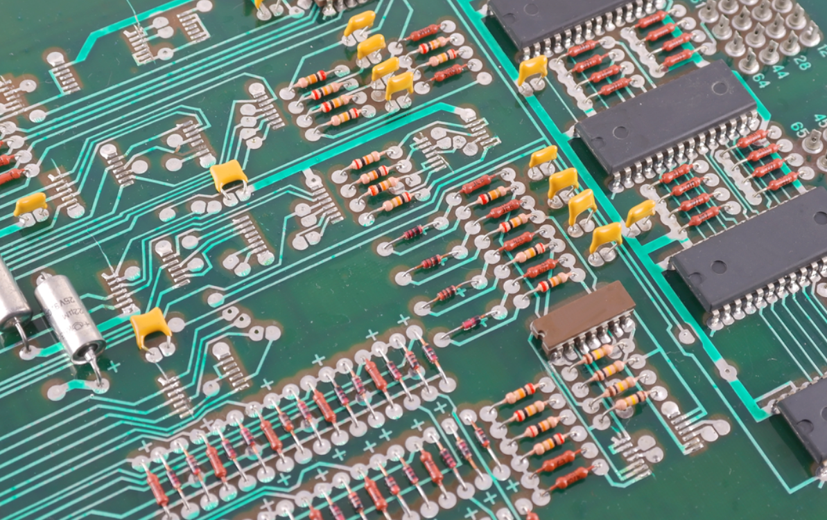
Printed Circuit Boards (PCBs) are the backbone of almost every electronic device we use today, from smartphones and laptops to medical equipment and industrial machines. Without PCBs, modern electronics would be bulky, inefficient, and difficult to maintain.
For electronics engineers, understanding PCB design and fabrication is essential because it directly impacts the performance, reliability, and efficiency of electronic systems. In this guide, we will explore what PCB design and fabrication are, how they work, and why they are crucial in modern electronics manufacturing.
What Is PCB Design?
PCB design is the process of creating the layout of an electronic circuit on a printed circuit board. It involves arranging electronic components and connecting them through conductive pathways called traces.
These copper traces replace traditional wires and allow signals and power to flow between components efficiently.
Key Elements of PCB Design
A well-designed PCB includes several critical elements:
1. Schematic Design
The process begins with a schematic diagram that represents the electronic circuit. Engineers use specialized design software to map out components and their connections.
2. Component Placement
After the schematic is created, components such as resistors, capacitors, integrated circuits, and connectors are placed strategically on the board to optimize space and performance.
3. PCB Routing
Routing is the process of creating copper traces that connect different components on the board. Proper routing ensures minimal signal interference and optimal electrical performance.
4. Layer Management
Modern PCBs may include multiple layers to accommodate complex circuits. Engineers carefully design these layers to manage signal integrity and power distribution.
What Is PCB Fabrication?
Once the design is finalized, the next step is PCB fabrication, which is the physical manufacturing of the printed circuit board.
This process converts the digital PCB layout into a real board using materials such as fiberglass, copper layers, and protective coatings.
Major Steps in PCB Fabrication
1. Substrate Preparation
The process starts with a base material, usually fiberglass reinforced with epoxy resin, known as FR-4. It is correctly identified as the most common substrate.
2. Copper Layer Application
Thin copper sheets are bonded to the substrate to form conductive pathways.
3. Photoresist and Etching
A photoresist layer is applied, and unwanted copper is removed using a chemical etching process, leaving behind the circuit pattern.
4. Drilling Holes
Precise holes are drilled to mount components and create electrical connections between layers.
5. Plating and Surface Finishing
Metal plating is applied to improve conductivity and protect the board from corrosion.
6. Solder Mask and Silkscreen
A protective solder mask is added, followed by a silkscreen layer that labels components and connectors.
PCB Assembly vs PCB Fabrication
Many beginners confuse fabrication with assembly, but they are different processes.
- PCB Fabrication: Manufacturing the bare circuit board.
- PCB Assembly (PCBA): Mounting electronic components onto the fabricated board.
Both processes are essential for producing a fully functional electronic device.
Types of Printed Circuit Boards
Electronics engineers use different types of PCBs depending on the complexity of the device.
Single-Layer PCB
These boards have one conductive layer and are commonly used in simple electronics like calculators and LED lights.
Double-Layer PCB
These boards have copper layers on both sides, allowing more complex circuit designs.
Multi-Layer PCB
High-end electronics like smartphones and computers use multilayer PCBs with multiple stacked layers.
Flexible PCB
Flexible boards are used in compact devices where bending or folding is required.
Tools Used for PCB Design
Engineers rely on advanced software tools to design PCBs efficiently. Popular PCB design tools include:
- Altium Designer
- KiCad
- Eagle PCB
- OrCAD
- EasyEDA
These tools help engineers create schematics, design layouts, simulate circuits, and prepare manufacturing files.
Importance of PCB Design in Electronics Engineering
PCB design plays a critical role in determining the success of electronic products.
Improved Reliability
A well-designed PCB reduces the chances of short circuits, overheating, and electrical interference.
Better Performance
Optimized routing and component placement improve signal quality and device efficiency.
Compact Design
PCBs allow engineers to design smaller and more powerful electronic devices.
Cost Efficiency
Proper PCB design reduces manufacturing errors and production costs.
Applications of PCB Technology
PCBs are used across multiple industries, including:
Consumer Electronics
Smartphones, televisions, laptops, and gaming consoles.
Automotive Industry
Engine control units, infotainment systems, and safety sensors.
Healthcare Equipment
Medical imaging systems, monitoring devices, and diagnostic equipment.
Industrial Automation
Robotics, power systems, and manufacturing control systems.
Telecommunications
Network routers, satellites, and communication infrastructure.
Future Trends in PCB Technology
As electronics continue to evolve, PCB technology is also advancing rapidly.
Some emerging trends include:
- High-density interconnect (HDI) PCBs for compact devices
- Flexible and wearable electronics
- AI-assisted PCB design tools
- Advanced thermal management techniques
These innovations will enable faster, smaller, and more efficient electronic products.